-
Email
-
WhatsApp
-
Address
Zhengzhou,Henan,China
Zhengzhou,Henan,China
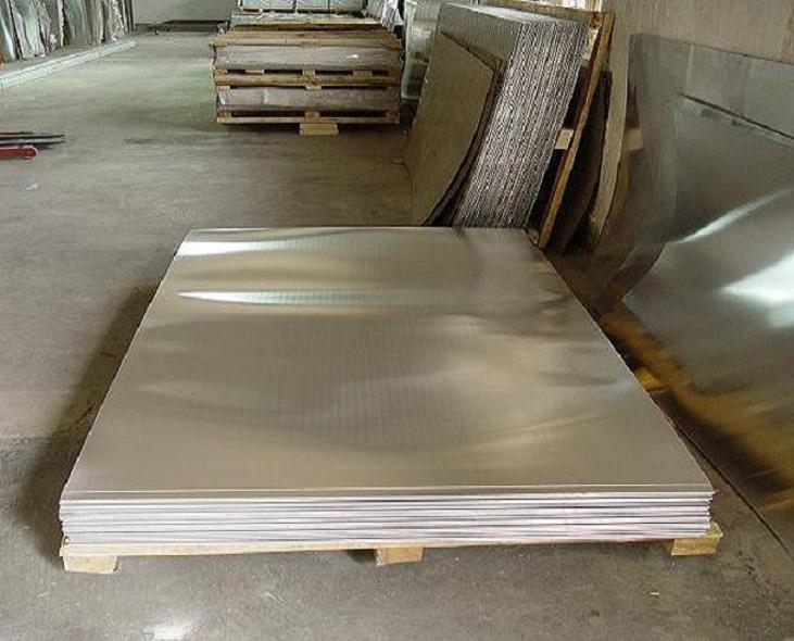
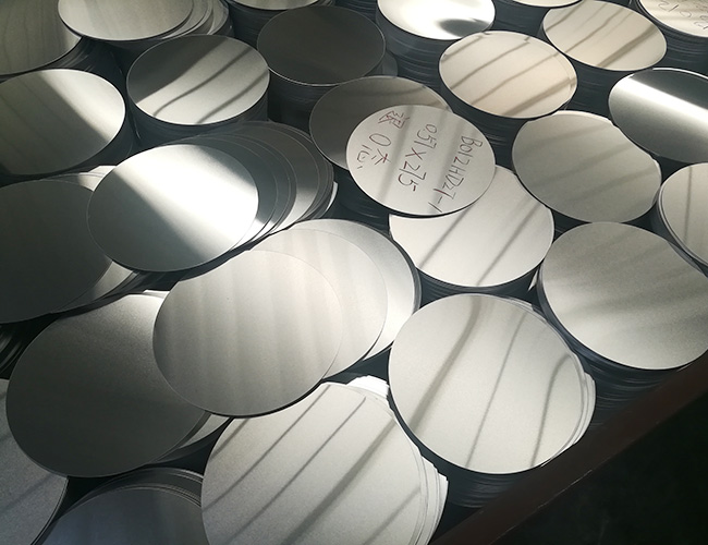
o h12 h14 h18 h24 aluminum aluminium disc for car. 1200 O H112 H12 H14 H24 Aluminum Circle Disc For Lamp Covered. Specifications: aluminium circle aluminium disc 1)Alloy: 1060 1070 1050 1100 1200 3003 3004 3105 5052 6061)Temper : O H12 H14 H16 H18 H22 H24 H26 H)Thickness:0.2mm-5mm 4)Diamters: 100mm---980mm Dimensions can be produced
1200 O aluminum circle disc wafer 15mm; Alloy 1000 3000 5000 Metal Circles With Good Price; Soft 0 5mm Thick Aluminum Blanks Circle Temper O H112; 1080 1060 3003 O H12 H14 H18 H24 Aluminum Coated Disc Prices; Hot Price 1050 1060 1070 3003 Hot Rolled Deep Drawing Aluminum Circle Blanks For Cookware With Cheap Price; 520mm Aluminum Discs 1100 ...
Nov 30, 2013 Vapox low temperature (400 o C) oxide glassivation. (Can handle 2u, 3u up to 8u wafers) Etching. Plasma and Wet etching of metal, silicon, poly, nitride, oxide. RIE etching of metal, silicon, nitride and oxide. Photo Lithography. We also do double sided aligning. Metal deposition of Al-Si 1% and Pure Aluminum on wafer. Doping
1 Principles of VLSI Design CMOS Processing CMPE 413 Silicon: Properties and Wafers Silicon in its pure or intrinsic state is a semiconductor, having bulk electrical resistance somewhere between a conductor and an insulator. Conductivity of silicon can be increased by several orders of magnitude by adding impurity atoms into the silicon lattice structure.
A specific example for an ALD process is the deposition of aluminum oxide, this can be realized with trimethylaluminum (TMA, C 3 H 9 Al) and water (H 2 O). First step is the elimination of hydrogen atoms which are bound to oxygen at the wafer surface. The methyl groups (CH 3) of TMA can react with the hydrogen to form methane (CH 4). The ...
o a D e (Equation 8.4) where D o denotes the diffusion coefficient extrapolated to infinite temperature and E a stands for the Arrhenius activation energy. For interstitial diffusion, E a is related to the energy required to move a dopant atom from one interstitial site to another. The values of E a are between 0.5 to 1.5 eV in both Si and GaAs.
Above the silicon, Qorvo deposits aluminum nitride and other films, which form a piezoelectric layer that acts as an acoustic resonator, filtering out unwanted frequencies. The goal is to pass on 100% of the in-band frequency. "This is not like GaAs or silicon where the active component is in the wafer. What we do is all up above the silicon.
A passively athermalized infrared imaging system includes an object side meniscus lens that forms at least one aspheric surface, and an image side meniscus lens that forms two aspheric surfaces. Each of the meniscus lenses are formed of a material selected from the group consisting of a chalcogenide glass, germanium, silicon, gallium arsenide, zinc selenide and glass.
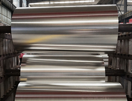
1060 3003 Zhongxin 1070 extruded aluminum wafer / slug for deep stamping. ... 1050 1060 1100 1200 aluminum circle discs. 1060 Aluminum disc bread for machine bread maker. Country/Region: China. Main Products: aluminum circle,aluminum coil,aluminum sheet,aluminum tread plate,aluminum strip.
White alumina powder F1200 mesh is an excellent polishing powder for stainless steel, aluminum alloy, copper, glass, and other materials. White fused aluminum oxide powder from us is an electrofused aluminum oxide powder. It is an aggressive grinding powder with high hardness, good toughness. White alumina powder F1200 mesh is an excellent polishing powder for
Dimensional Data – Wafer and Lug. Dimensional Data – Gear Operator. Performance Features and Technical Information. Valve Seating Torques and Technical Information. Product Options – Actuation. Disc and Seat Material Data. Sure Flow Equipment Inc. Toll Free Tel: 1-800-263-8251.
Nov 25, 2021 Hot forming aluminum processes are important for many industrial sectors such as aerospace and automobiles. However, these processes can face challenges. ... (up to 1200 o C) ... ® DI optical surface inspection tool for semiconductor applications enables inspection of structured and unstructured wafers during the entire manufacturing process.
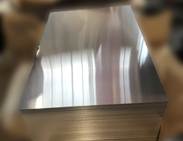
Our Aluminum disc shaped aluminium sheet have many types of alloy,such as alloy grade 3003、AA 1050、alloy 1070 A1050 O、AA 1100 3003 1060 1200 HO alloy,also have AA3003 deep drawing quality hard anodising quality、alloy 3003 DDQ hard anodizing、alloy 3003 H12、3003 O temper hard anodized quality、1100 3003 anodized quality、alloy 1100 ...
1 Principles of VLSI Design CMOS Processing CMPE 413 Silicon: Properties and Wafers Silicon in its pure or intrinsic state is a semiconductor, having bulk electrical resistance somewhere between a conductor and an insulator. Conductivity of silicon can be increased by several orders of magnitude by adding impurity atoms into the silicon lattice structure.
A specific example for an ALD process is the deposition of aluminum oxide, this can be realized with trimethylaluminum (TMA, C 3 H 9 Al) and water (H 2 O). First step is the elimination of hydrogen atoms which are bound to oxygen at the wafer surface. The methyl groups (CH 3) of TMA can react with the hydrogen to form methane (CH 4). The ...
800 900 1000 1100 1200 1300 Fig. 8. Solid solubility of dopants in Si (Ref: Plummer Griffin, Proc. IEEE, April 2001) Barrier Height Figure: 9 Accumulation and depletion type contacts. pc is the physical parameter that describes the transport of majority carriers across heavily doped Si-metal interfaces.
O 3 and intergranular glass in 85 to 98% alu-mina compositions, SiC and silicon in reaction-bonded silicon carbide, and between adjacent grains of MgAl 2 O 4 spinel. Relief polishing can also polish the metal components in cross sections of microelectronic devices. Vibratory polishing with colloidal silica or alumina slurry, step 5(b) in
Aug 18, 2021 After the cleaning is completed, the wafer can be placed in a high temperature environment of 800 to 1200 degrees Celsius, and a layer of silicon dioxide is formed by the flow of oxygen or vapor on the wafer surface. ... After the wafer enters the vacuum state, the thin film formed by aluminum particles will adhere to the wafer. This process is ...
PURPOSE: A porous chuck for fixing a semiconductor wafer with a vacuum state is provided to prevent the leakage of vacuum suction power by surrounding a porous ceramic using a frame. CONSTITUTION: A frame(1100) comprises a plurality of vacuum holes and an exhaust groove on the bottom thereof. The frame comprises a circular partition(1300) on the edge of a disk.
1200 Aluminum Non-alloy Sheet With All DDQ Material 1200 O H14 H24 Aluminum Circle For Pressure Flat Aluminum Circle 3003 Manufacturer - Quick Details Grade: 1000 Series Temper: O-H112 Type: Plate Application: Reflective Sign Boards Road Furniture Utensils Sand witch Bottom Thickness: 0.36--4.0mm Width: 100 --1200 mm Surface Treatmen Coated Alloy Or No
May 30, 2020 Both 1100-O aluminum and 1200-O aluminum are aluminum alloys. Both are furnished in the annealed condition. Their average alloy composition is basically identical. There are 31 material properties with values for both materials. Properties with values for just one material (1, in this case) are not shown.
Wafer Butterfly Valve With Aluminum Handlever DN50-DN1200 Industrial Use The butterfly valves are widely used in piping of chemical, food, medicine, paper making, water and electricity, shipbuilding, water supply and drainage, metallurgy and energy systems, and is available for regulating and closure devices in a variety of corrosive, non ...
Nov 25, 2021 Hot forming aluminum processes are important for many industrial sectors such as aerospace and automobiles. However, these processes can face challenges. ... (up to 1200 o C) ... ® DI optical surface inspection tool for semiconductor applications enables inspection of structured and unstructured wafers during the entire manufacturing process.
Our Aluminum disc shaped aluminium sheet have many types of alloy,such as alloy grade 3003、AA 1050、alloy 1070 A1050 O、AA 1100 3003 1060 1200 HO alloy,also have AA3003 deep drawing quality hard anodising quality、alloy 3003 DDQ hard anodizing、alloy 3003 H12、3003 O temper hard anodized quality、1100 3003 anodized quality、alloy 1100 ...
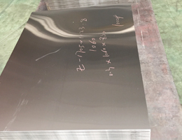
Aluminium Alloy 1200 Foil, Sheet and Plate, Aluminum Alloy 1200 Bar / Rod and Wire, Alloy 1200 is also available in Drawn Tube, Solid Conductor. For all stock availability for Aluminium Alloy 1200 contact Sales. Specifications Similar Specifications: 6L16, Alloy 1200 sheet and strip H14 or H24 6L17, Alloy 1200 sheet and strip O Temper
3. Partial pressure of oxidizing species ( No) •Also dependent on: 4. Reactant type: Dry O2 Water vapor faster oxidation, since water has a higher solubility (i.e., D) in SiO2 than O2 5. Crystal orientation: <111> faster, because there are more bonds available at the Si-surface <100> fewer interface traps; smaller # of
*Reference: IOFFE. SiC 4H and SiC 6H manufacturer reference: PAM-XIAMEN is the world's leading developer of solid-state lighting technology,he offer a full line: Sinlge crystal SiC wafer and epitaxial wafer and SiC wafer reclaim. [This information has already been had a
6000 Å aluminum + 5500 Å thermal oxide = 11000 Å. Probe Depth = 10000Å. Blanket aluminum wafer from IMSI SEMATECH. Miller, et al., SWTW-2007. Background – – Height Effects • Pad material pile-up has also been correlated to ... - 1200. Metal Thickness. nm. Courtesy of Infineon. Probe Needle Design Changes
Wafer Semi-Lug Lug F B S::: Flanged Butt Welding Socket Type D - Operation L G C E P F H O::::: Lever Gear Chain Wheel ... ALUMINUM / ALUMINUM BRONZE DUCTILE IRON(+NICKEL PLATED) CARBON STEEL(+NICKEL PLATED) SS304 / SS316 / ALUMINUM BRONZE. inch SIZE ... 1100 1200 1300 1400 1600 1800 40 52 64 76 101 126 149 196 244 294 333 384 435
Wafer cassette systems and methods of using wafer cassette systems. A wafer cassette system can include a base and a probe card assembly. The base and the probe card assembly can each include complementary interlocking alignment elements. The alignment elements can constrain relative movement of the base and probe card assembly in directions parallel to a wafer
Fig. 13.7A illustrates the chemical polishing mechanism. A part of steel material has been progressively removed and the steel ball is truncated at the end (see schematic in Fig. 13.7B).The roughness inside the wear scar measured by atomic force microscopy indicates the existence of Ra values below 1 nm sub-nm Ra values. Compared with lubricant film thickness calculations
May 30, 2020 1200-O aluminum is 1200 aluminum in the annealed condition. It has the second lowest strength and highest ductility compared to the other variants of 1200 aluminum. The graph bars on the material properties cards below compare 1200-O aluminum to: 1000-series alloys (top), all aluminum alloys (middle), and the entire database (bottom).
Wafer Butterfly Valve With Aluminum Handlever DN50-DN1200 Industrial Use The butterfly valves are widely used in piping of chemical, food, medicine, paper making, water and electricity, shipbuilding, water supply and drainage, metallurgy and energy systems, and is available for regulating and closure devices in a variety of corrosive, non ...
Our Aluminum disc shaped aluminium sheet have many types of alloy,such as alloy grade 3003、AA 1050、alloy 1070 A1050 O、AA 1100 3003 1060 1200 HO alloy,also have AA3003 deep drawing quality hard anodising quality、alloy 3003 DDQ hard anodizing、alloy 3003 H12、3003 O temper hard anodized quality、1100 3003 anodized quality、alloy 1100 ...
6000 Å aluminum + 5500 Å thermal oxide = 11000 Å. Probe Depth = 10000Å. Blanket aluminum wafer from IMSI SEMATECH. Miller, et al., SWTW-2007. Background – – Height Effects • Pad material pile-up has also been correlated to ... - 1200. Metal Thickness. nm. Courtesy of Infineon. Probe Needle Design Changes
Nov 22, 2021 Epitaxial AlN films on c-sapphire are today the most widespread pseudo-substrates to produce AlGaN-based UV light-emitting devices. The large lattice mismatch between AlN and α-Al 2 O 3, however, causes a high density of threading dislocations that negatively impact the performance of optoelectronic devices.Thermal annealing at 1500–1700
Lab Report on Schottky Diode Fabrication of 1st Semester of M-Tech in VLSI Microelectronics Back side metalisation: Back side of the wafer Ag metalized same as above or coating a silver paste with paint brush. After that heat treatment is required at 110 OC for 10 minute and 700 OC for 45 second.If the backside coating is silver paste then it
The present invention is a novel cleaning method and a solution for use in a single wafer cleaning process. According to the present invention the cleaning solution comprises ammonium hydroxide (NH 4 OH), hydrogen peroxide (H 2 O 2 ), water (H 2 O) and a chelating agent. In an embodiment of the present invention the cleaning solution also contains a surfactant.
ASTM B209 specification covers aluminum and aluminum-alloy flat sheet, coiled sheet, and plate in the alloys (Note 1) and tempers shown in Tables 2 and 3, and in the following finishes: (A) Limits are in weight percent maximum unless shown as a range or stated otherwise. (B) Analysis shall be made for the elements for which limits are shown in this table.
•Bare Si before and after each wafer •Monitor etch conditions using OES •Analysis of data •Baseline fingerprint of materials relevant to the etch •Identify useful wavelengths 7. MET setup •x2 2-meter Fiber Patch Cables from Thorlabs with range 200-1200 nm ... 1200 1400 1600
Pre-oxidation Wafer Clean Particulate Removal • Strong oxidants remove organic residues. •H2SO4:H2O2 or NH3OH:H2O2 followed by DI H2O rinse. • High pressure scrub or immersion in heated dunk tank followed by rinse, spin dry and/or dry bake (100 to 125 ꉘC). Pre-oxidation Wafer Clean Organic Removal