-
Email
-
WhatsApp
-
Address
Zhengzhou,Henan,China
Zhengzhou,Henan,China
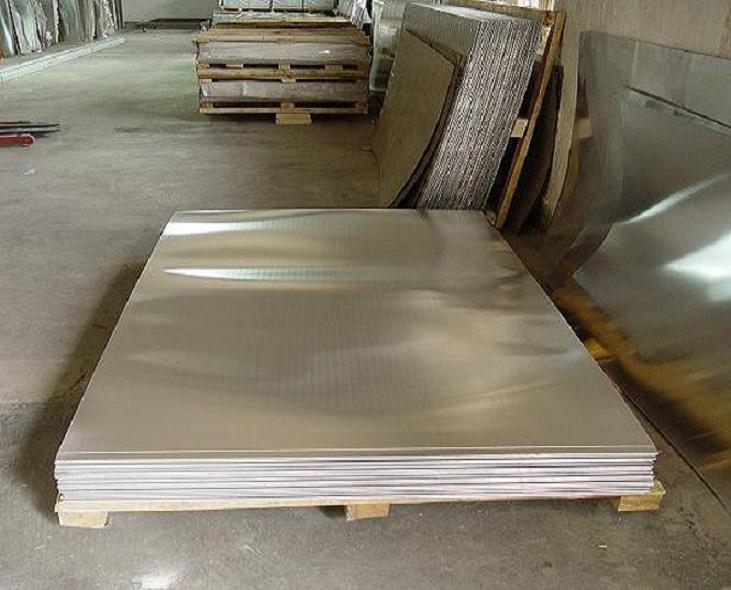
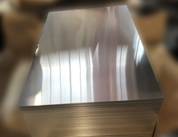
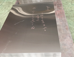
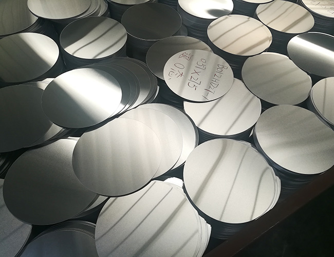
The common specification of aluminum wafer which manufactured on the market are the alloys of 1050, 1060, 1070, 1100 and 3003, the temper are O, H12 and H14, the thickness is 0.4-5.0mm, and the diameter is 20-1200mm. Some companies will encounter some of the above problems when purchasing aluminum wafers.
The Aluminum Nitride (AlN) Wafer Market 2021 report covers an analytical view with complete information of product types, sales and revenue by region, including manufacturing cost analysis, industrial chain and market effect factors analysis. The report covers the market landscape and its growth prospects over the coming years.
Aug 03, 2021 Geographically, global Aluminum Nitride (AlN) Wafer Market has been scrutinized across global regions to study about various successful strategies carried out by industries. It includes major regions such as North America, Latin America, Middle East, Asia-Pacific, Africa, and Europe on the basis of different parameters.
1 天前 Edison, NJ -- -- 01/03/2022 -- The Solar Ingot Wafer Market has witnessed continuous growth in past few years and is projected to grow at good pace during the forecast period of 2022-2027.The exploration provides a 360° view and insights, highlighting major outcomes of Solar Ingot Wafer industry. These insights help the business decision-makers to formulate better
Global “Wafer Fabrication Materials Market" is expected to grow at a steady growth during the forecast period 2021-2026, Wafer Fabrication Materials Market report offers insights into the latest trends.It summarizes key aspects of the market, with focus on leading key player's areas that have witnessed the highest demand, leading regions and applications.
1 天前 Edison, NJ -- -- 01/03/2022 -- The Solar Ingot Wafer Market has witnessed continuous growth in past few years and is projected to grow at good pace during the forecast period of 2022-2027.The exploration provides a 360° view and insights, highlighting major outcomes of Solar Ingot Wafer industry. These insights help the business decision-makers to formulate better
The global gallium arsenide (GaAs) wafer market is expected to grow at a CAGR of 12.5% during the forecast period (2021 - 2026). GaAs wafers are preferred over silicon and other compound semiconductor devices because of better functionality, scalability, and compatibility with the IoT network.
Dec 22, 2021 The Omicron variant of COVID-19 has acted as a speedbump of sorts in growth revival which had picked momentum from the second half of 2021. However, come 2022, the expectation is that industries will tide over this crisis and therefore the demand for aluminium is bound to increase as electronics, automobile, packaging industries pick steam. The demand
1 天前 Players, stakeholders, and other participants in the global Indium Phosphide (InP) Wafers market will be able to gain the upper hand as they use the report as a powerful resource. The segmental analysis focuses on sales, revenue and forecast by region (country), by Type and by Application for the period 2016-2027. Segment by Type.
The global semiconductor glass wafer market is expected to grow at a compound annual growth rate of 5.84% over the analyzed period to reach a market size of US$530.472 million in 2026 from US$356.472 million in 2019. Semiconductor glass wafer is circular pieces of precision glass that are used in various technical and industrial manufacturing.
Global Semiconductor Materials Market : Industry Analysis and Forecast (2020-2027)-By Material Type, End-Users, and Region. The Global Semiconductor Materials Market was valued US$ 51.32 Bn in 2019 and is expected to reach 58.43 Bn by 2027, at a CAGR of 5.52% during the forecast period. To know about the Research Methodology :- Request Free ...
Elements from the periodic table of the alumina wafer are printed on a single layer of silicon wire on the top of an aluminum template. Elements in the periodic table of alumina wafers printed in a one-atom-thick layer on an aluminum template (Figure A). The Element Periodic Tables of aluminium wafers are prints in a 1.5 by 1.6 metre layer.
Almost all Earth Materials are used by humans for something. The Aluminum Wafer manufacturers proovide Refractory Materials, Aluminum Disc, Silicon Carbide products with 1. These products can be used for different uses such as making machines, making roads and buildings, or making computer chips and concrete, ceramics,
Largest Market: Asia Pacific. CAGR: 7.9 %. Key Players. A thin wafer is a thin piece of semiconductor material used for integrated circuit manufacturing. One of the main factors supporting the growth of the thin wafer market is the rising demand for semiconductor devices in sectors, such as automotive, consumer electronics, and telecommunications.
Global “Wafer Fabrication Materials Market" is expected to grow at a steady growth during the forecast period 2021-2026, Wafer Fabrication Materials Market report offers insights into the latest trends.It summarizes key aspects of the market, with focus on leading key player's areas that have witnessed the highest demand, leading regions and applications.
The global gallium arsenide (GaAs) wafer market is expected to grow at a CAGR of 12.5% during the forecast period (2021 - 2026). GaAs wafers are preferred over silicon and other compound semiconductor devices because of better functionality, scalability, and compatibility with the IoT network.
Global Thin Wafer Market was valued at US$ 7.72 Bn in 2019 and is expected to reach 10.60 Bn by 2027, at a CAGR of 4.63 % during the forecast period. The report includes an analysis of the impact of COVID-19 lockdown on the revenue of market leaders, followers, and disruptors.
A majority of LEDs are grown on sapphire wafers. Monocrystal was the first company to introduce 6-, 8- and 10-inch sapphire wafers to the market, in anticipation of the industry trends. Now the company holds a leading position on 6- and 8-inch wafer market. The key LED parameters depend on the surface quality of a sapphire substrate.
Global Semiconductor Materials Market : Industry Analysis and Forecast (2020-2027)-By Material Type, End-Users, and Region. The Global Semiconductor Materials Market was valued US$ 51.32 Bn in 2019 and is expected to reach 58.43 Bn by 2027, at a CAGR of 5.52% during the forecast period. To know about the Research Methodology :- Request Free ...
Indium Phosphide (InP) Wafers Market Size And Forecast. Indium Phosphide (InP) Wafers Market was valued at USD 84.85 Million in 2019 and is projected to reach USD 236.82 Million by 2027, growing at a CAGR of 13.7% from 2020 to 2027.. The demand for high speed internet connectivity in variety of datacom and telecom applications will upsurge the demand for indium
Global Aluminum Nitride (AlN) Wafer Market Research Report contains Market Size, Market Share, Market Dynamics, Porter's 5 force Analysis, Segmentation, Regional and Competitor Analysis. Pages: 105, Tables Figures: 122, Published-date: Aug-27-2021, Price: Single User = $2900. Product: Aluminum Nitride (AlN) Wafer, Product-Type: 2 Inch, 4 Inch, Others,
Almost all Earth Materials are used by humans for something. The Aluminum Wafer manufacturers proovide Refractory Materials, Aluminum Disc, Silicon Carbide products with 1. These products can be used for different uses such as making machines, making roads and buildings, or making computer chips and concrete, ceramics,
Elements from the periodic table of the alumina wafer are printed on a single layer of silicon wire on the top of an aluminum template. Elements in the periodic table of alumina wafers printed in a one-atom-thick layer on an aluminum template (Figure A). The Element Periodic Tables of aluminium wafers are prints in a 1.5 by 1.6 metre layer.
The 200 mm thin wafer held 40% of the market share in 2020 and will grow at a CAGR of around 7.50% through 2027. 200 mm wafers are experiencing a rising adoption among the market leaders of power devices such as Metal-Oxide-Semiconductor Field-Effect Transistor (MOSFET), Insulated-Gate Bipolar Transistor (IGBT), and Radio Frequency (RF) devices.
Global semiconductor wafer market share has been valued at which is expected to grow at the US $40 billion by the end of the forecast period with CAGR of 3.8%. Asia-Pacific represented the biggest pieces of the overall industry with a market estimation of USD 4,371.2 million every 2019, trailed by North America and Europe.
The global gallium arsenide (GaAs) wafer market is expected to grow at a CAGR of 12.5% during the forecast period (2021 - 2026). GaAs wafers are preferred over silicon and other compound semiconductor devices because of better functionality, scalability, and compatibility with the IoT network.
Semiconductor Wafer Cleaning Equipment Market Size And Forecast. Semiconductor Wafer Cleaning Equipment Market size was valued at USD 5,880.28 Million in 2020 and is projected to reach USD 11,828.98 Million by 2028, growing at a CAGR of 9.95% from 2021 to 2028.. Growing penetration of printed electronics and rising concern for upgrading and enhancing the
Solar Grade Wafer market is segmented by Type, and by Application. Players, stakeholders, and other participants in the global Solar Grade Wafer market will be able to gain the upper hand as they use the report as a powerful resource. ... Calcined Aluminum Oxide Powder Market Size By Types( Standard Calcined Alumina, Tabular Alumina, White ...
Silicon Wafers Market can capitalize with an impressive CAGR of 3.19% and be valued, worth USD 11,889.0 Million by 2027, Global Silicon Wafers Market Report categorizes the Global Market by Type, by End-Use and Region Silicon Wafers Industry
Dec 16, 2021 Silicon Wafer Market Demand, Industry Analysis, Growth, Applications, Types and Forecasts Report 2028. by Emergen Research December 16, 2021. A new market assessment report on Silicon Wafer Market brings to light a detailed statistics on the dramatic shift in the competitive landscape and business environment of the Silicon Wafer Market for ...
Market Analysis and Insights : Global Wafer Level Packaging Market. Wafer level packaging market will expect to grow at a rate of 21.0% for the forecast period of 2021 to 2028. Wafer level packaging market report analyses the growth, which is currently being growing due to the impending need for circuit miniaturization in microelectronic devices.